


Samsung to Make Nvidia HBM4E Base Dies on TSMC’s 3nm Process
 20 October 2026 05:37 PM
Summary: Samsung Electronics will reportedly use TSMC’s 3nm process to manufacture logic base dies for Nvidia’s custom HBM4E memory, marking a first-of-its-kind collaboration aimed at standardizing production across suppliers.
Samsung Electronics will manufacture the logic base die for Nvidia’s custom high-bandwidth memory (HBM) using Taiwan Semiconductor Manufacturing Co.’s (TSMC) 3nm process, according to Seoul Economic Daily, citing industry sources. The move would mark the first time Samsung and Nvidia have collaborated on HBM production.

Nvidia reportedly wants its three HBM suppliers—Samsung, SK Hynix and Micron—to use the same 3nm process for base dies and its 1c DRAM node for memory dies. The strategy aims to improve consistency across suppliers and simplify qualification of Nvidia’s custom NVHBM architecture, which is based on HBM4E.
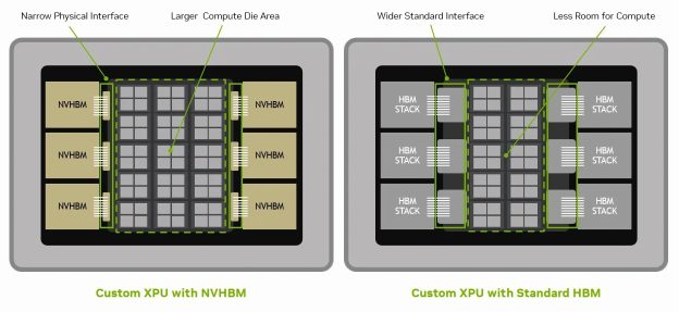
The design moves the memory controller from the GPU to the HBM base die, freeing space for additional computing circuits. According to the report, NVHBM could deliver up to 30% more bandwidth and 15% lower power consumption than standard HBM4E.
The collaboration comes as demand for high-bandwidth memory continues to rise. UBS estimates that HBM demand will reach 61.5 billion gigabits next year, up 91% year over year, while projected shipments total 54.6 billion gigabits—a potential supply gap of about 10%.
Samsung is expected to retain its turnkey manufacturing model for standard HBM4 and HBM4E products and other custom-memory programs. The company is also reportedly evaluating whether its own foundry can manufacture Nvidia’s base die using its 2nm process, potentially providing an alternative if TSMC capacity becomes constrained.