


Abstract
Researchers have developed a diamond-based sensor using NV centers for high-precision detection of electric and magnetic fields at the nanoscale. With 500 nm spatial and 100 fs temporal resolution, it enables real-time monitoring of electric field dynamics, offering key insights for nanomaterials and quantum technologies.
Researchers from the University of Tsukuba have developed a groundbreaking method for sensing electric and magnetic fields at the nanometer scale, a key advance for quantum technologies and nanodevices. The team, led by Daisuke Sato, has engineered a diamond nonlinear photonic sensor using nitrogen-vacancy (NV) centers, enabling real-time monitoring of electric fields with extraordinary precision.
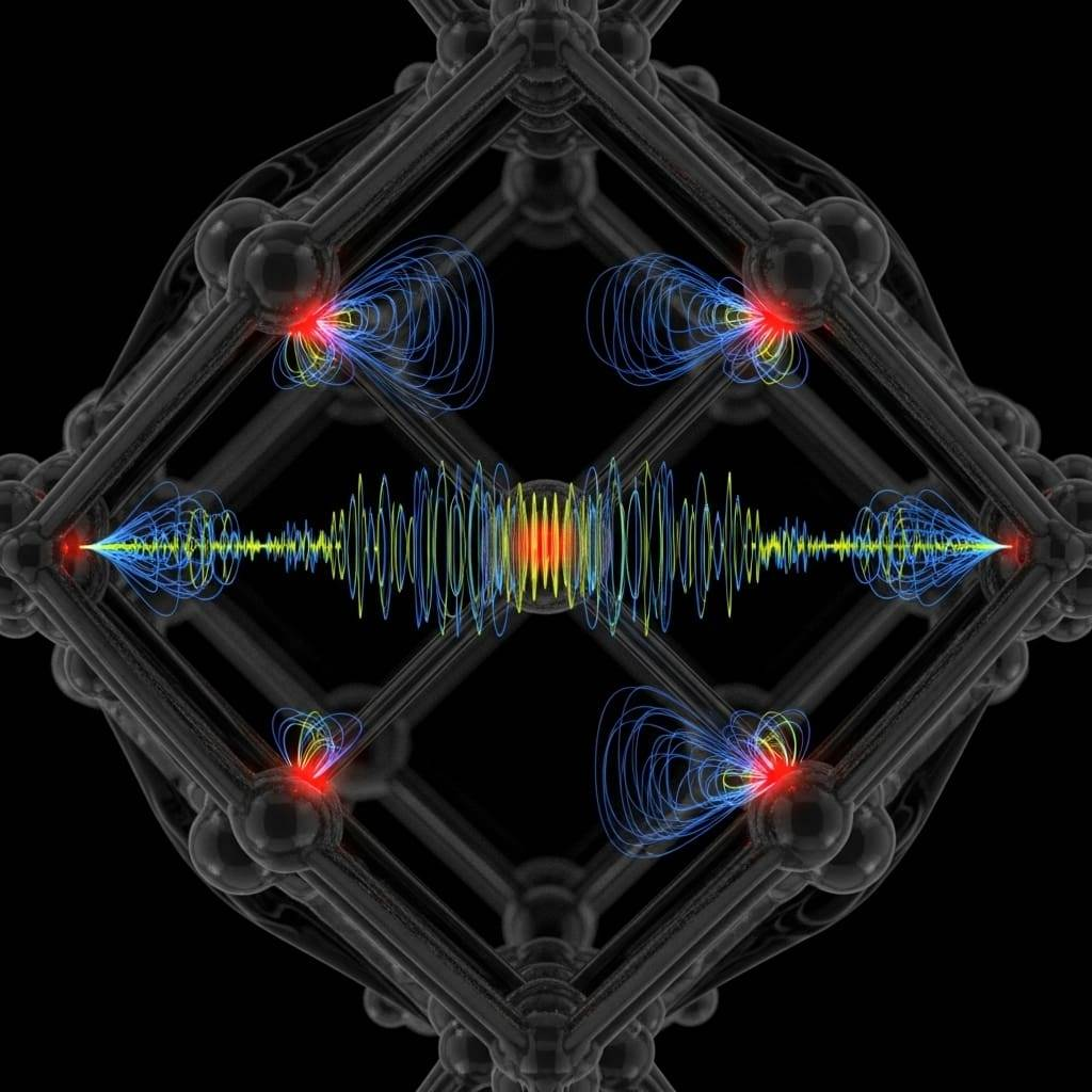
This new approach overcomes the limitations of traditional techniques by exploiting the Pockels effect in diamond NV centers, which allows non-resonant electric field modulation without the need for metallic contacts or external microwaves. The sensor achieves spatial resolutions of 500 nanometers and temporal resolutions of 100 femtoseconds, ideal for characterizing advanced nanomaterials and quantum devices.
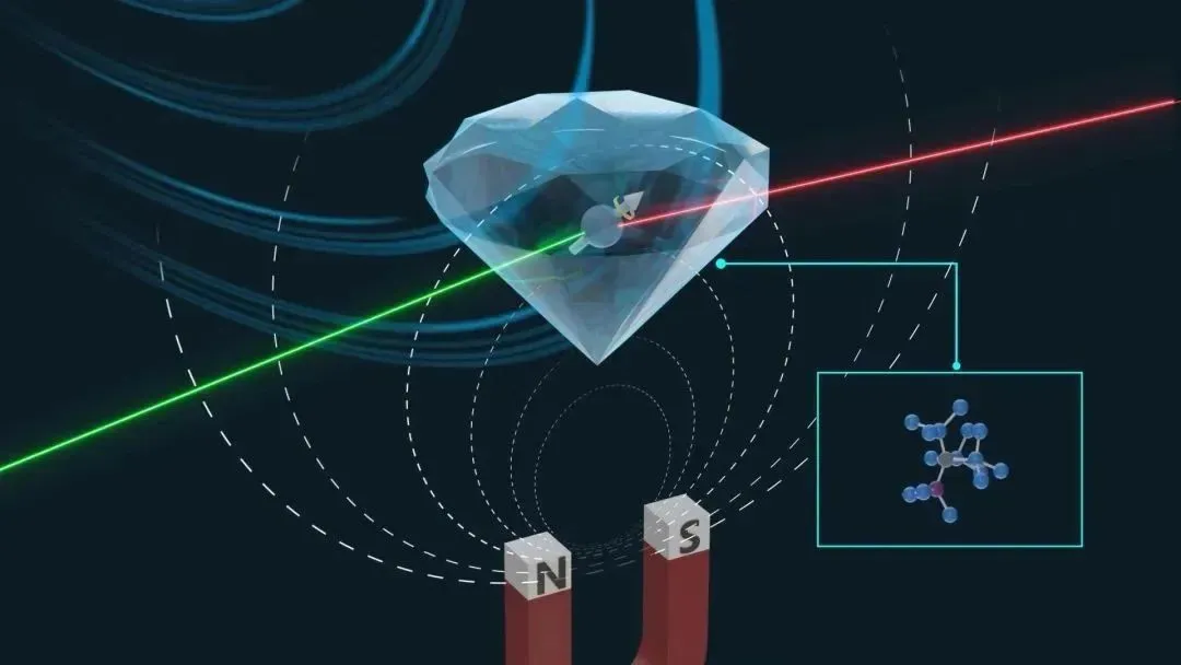
The sensor's high sensitivity was validated by detecting static and dynamic electric fields in test samples with remarkable accuracy. This breakthrough allows unprecedented mapping of electric field dynamics at ultrafast timescales, offering key insights into carrier scattering and surface phenomena.
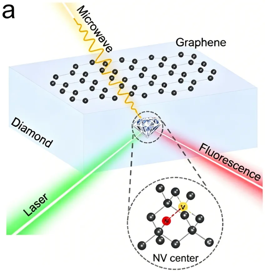
This diamond NV-based sensor is poised to play a critical role in the future of nanotechnology, semiconductor devices, and quantum systems, enabling precise, non-invasive field measurements for both research and industrial applications.

