


A new in-memory computing chip, developed by an international team including researchers from Politecnico di Milano, addresses the growing mismatch between processing power and energy consumption. Published in Nature Electronics, the chip combines energy efficiency and speed by co-locating data storage and computation, eliminating the need for constant data transfer between memory and processors.

Key Design Features
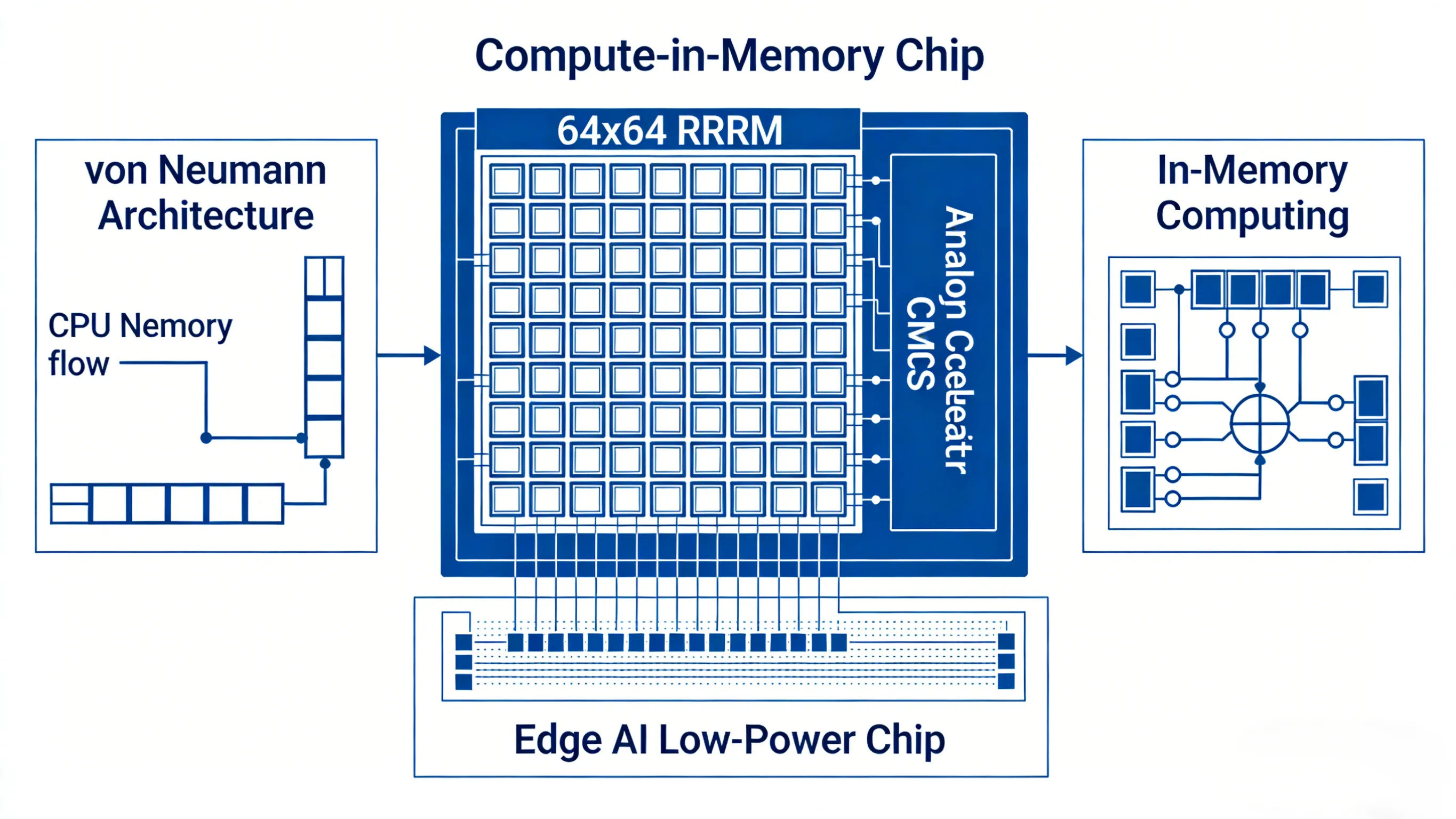
The chip uses an analog accelerator built with standard CMOS technology, featuring two 64×64 programmable resistive memory arrays. This allows the memory itself to perform computations, reducing power use and processing time. The system integrates key analog components like operational amplifiers and analog-to-digital converters, enabling it to solve both linear and nonlinear equations.
Performance and Potential
Experimental tests show that the chip matches digital systems in accuracy while offering lower energy consumption, faster computation, and a smaller footprint. This makes it ideal for energy-sensitive applications such as edge AI, robotics, and wireless infrastructure.
Future Applications
The chip’s design, compatible with existing semiconductor manufacturing, makes it suitable for large-scale production. Researchers aim to refine the technology for AI workloads and expand its use in data centers and 5G/6G systems.
This innovation signals a shift toward hybrid architectures that balance performance with energy efficiency in the next generation of computing.

