


A team of researchers from Peking University and the Chinese Academy of Sciences has unveiled the world’s smallest ferroelectric transistor, successfully reducing the gate length to just 1 nanometer. This breakthrough, published in Science Advances, allows the device to operate at a remarkably low voltage of just 0.6 volts, addressing a key power consumption challenge in semiconductor technology.
A computer chip
A Significant Leap in Power Efficiency
Modern logic chips typically operate efficiently at around 0.7 volts, but non-volatile memory technologies, such as NAND flash, often require voltages of 5 volts or more to perform write operations. Even previous ferroelectric field-effect transistors (FeFETs) needed over 1.5 volts. This voltage gap often necessitates complex step-up circuits, which consume valuable space and energy. In AI chips, for example, up to 90% of total power is spent on data transfer rather than computation.
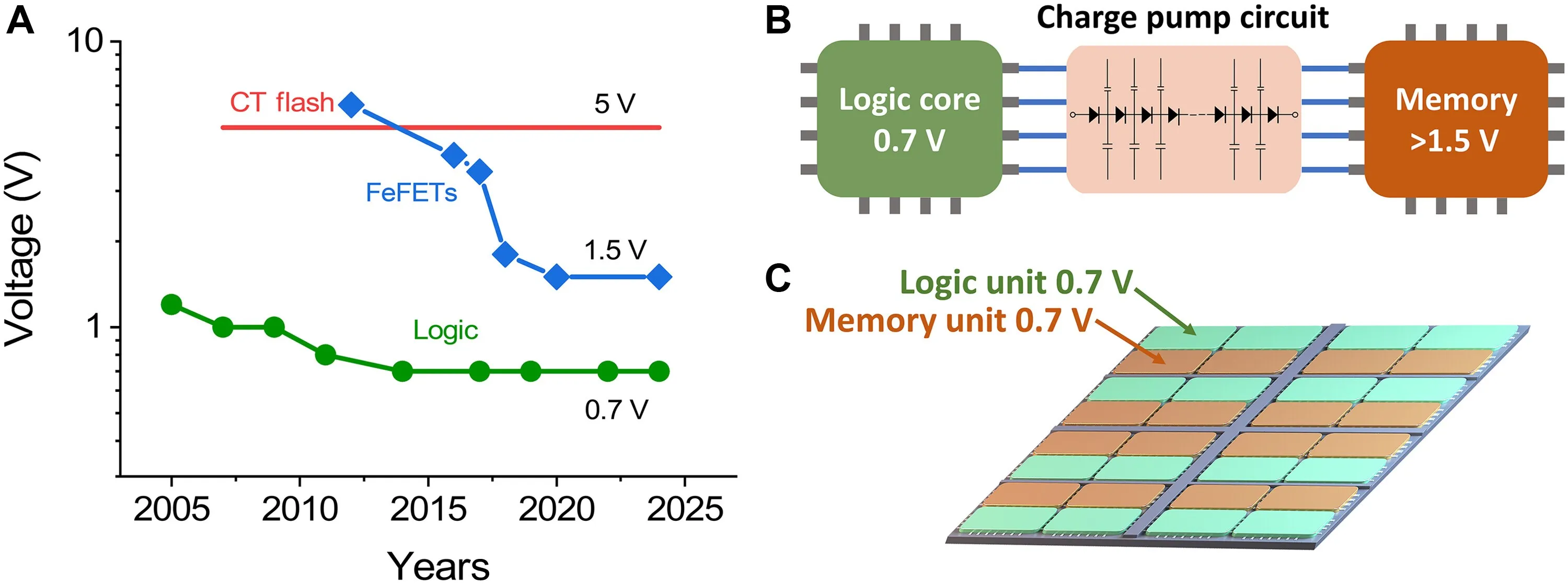
Voltage mismatch between logic core and memory.
To overcome this challenge, the research team, led by Qiu Chenguang and Peng Lianmao, utilized metallic single-walled carbon nanotubes as gate electrodes. This innovative design acts as a nanotip, which concentrates the electric field, improving the coupling between the ferroelectric layer and the transistor channel. This enhancement allows the device to flip its polarization state at just 0.6 volts, below the typical logic voltage, while remaining immune to short-channel effects.
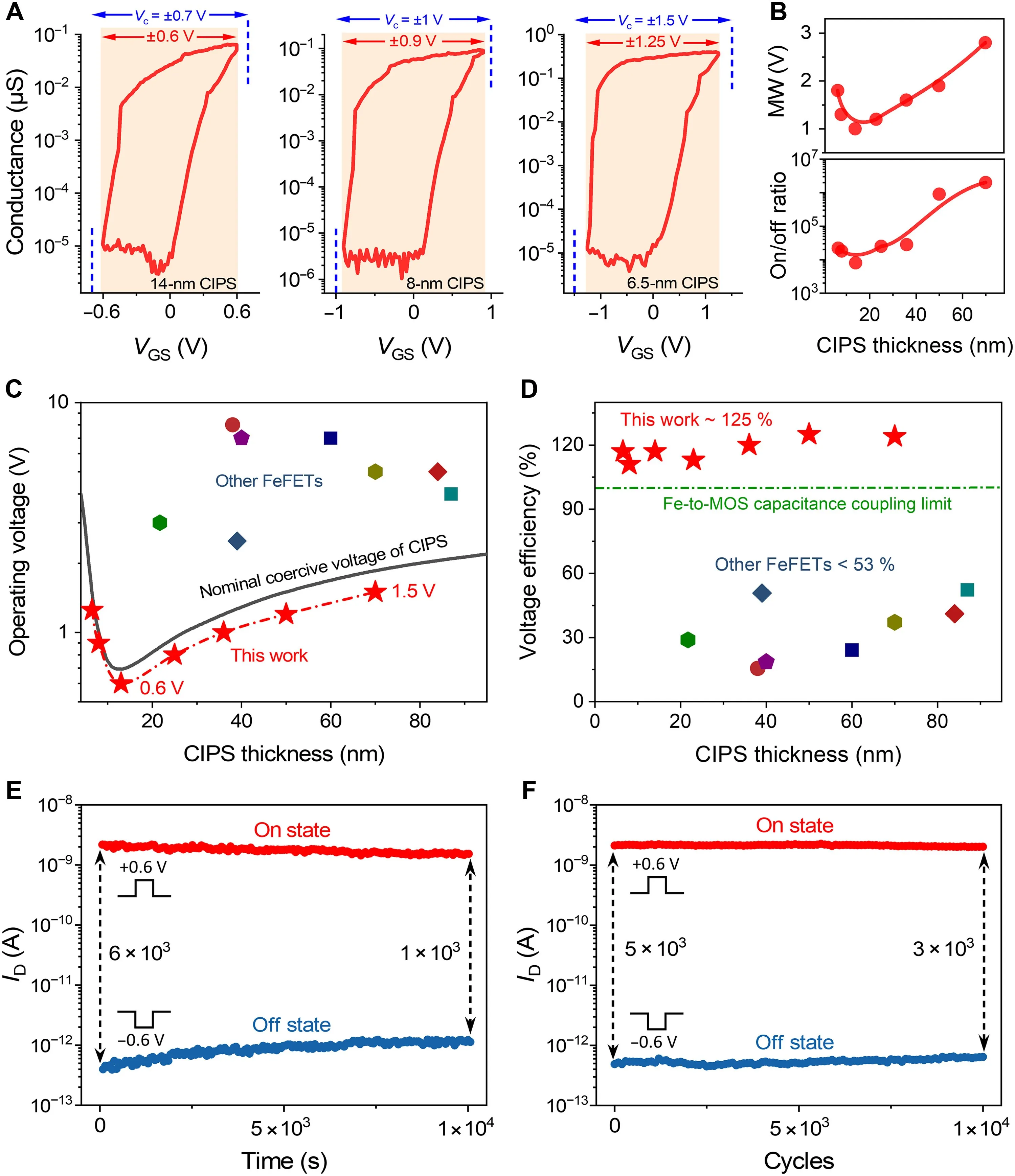
Nanogate MoS2 FeFETs with ultralow operating voltage exceeding the nominal coercive voltage.
Enhanced Memory and Performance
The new molybdenum disulfide (MoS2)-based FeFETs exhibit exceptional memory performance, with a current on/off ratio of 2 million and a fast programming speed of just 1.6 nanoseconds. By achieving voltage compatibility between memory and logic units, the device eliminates the need for additional charge pump circuits, streamlining high-speed data interaction.
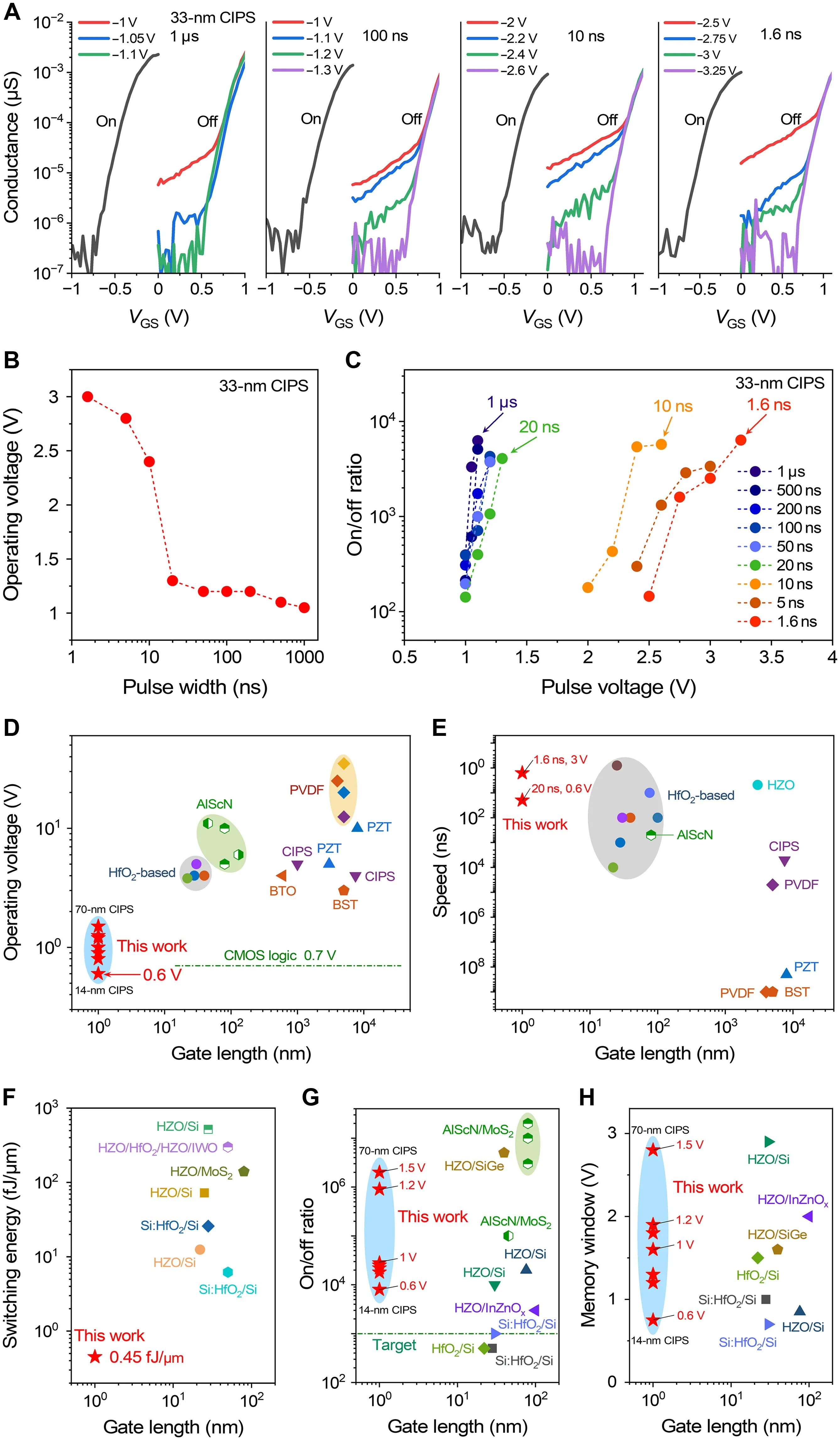
Operating speed and benchmark of our nanogate MoS2 FeFETs.
Implications for Future Technologies
This innovation not only reduces power consumption but also opens the door for more efficient integration between memory and logic circuits. The researchers note that the fundamental principles behind the design are compatible with mainstream ferroelectric materials and can be integrated into standard industrial manufacturing processes.
The breakthrough holds significant potential for the future of applications requiring high energy efficiency, such as large model inference, edge intelligence, and wearable devices. As the demand for energy-efficient solutions grows, this technology could play a crucial role in shaping the next generation of low-power electronics.

