


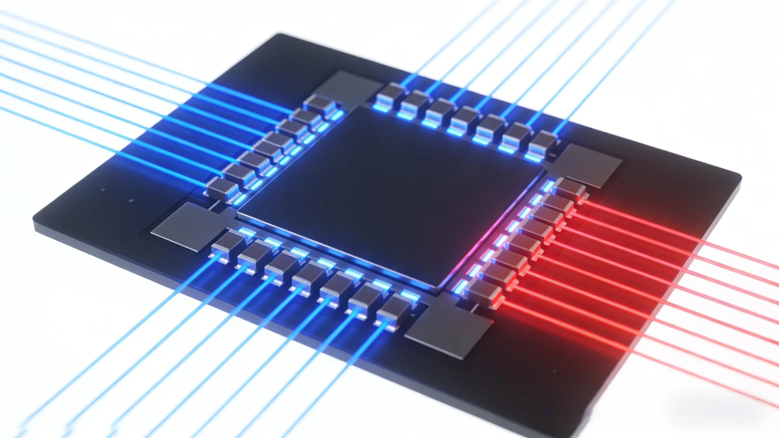
A revolutionary advancement in LED technology has led to the development of a single chip capable of emitting two distinct infrared wavelengths simultaneously. This breakthrough, which could transform applications in biodiagnostics, environmental sensing, and autonomous driving, was announced by the National Research Foundation of Korea. It was achieved through a collaboration between the Korea Research Institute of Standards and Science (KRISS), Stanford University, and Germany’s Helmholtz-Zentrum.
Traditional Challenges with Infrared LEDs
Historically, infrared LEDs emitted light in only one wavelength band. To cater to applications requiring different wavelengths, multiple LEDs were needed, leading to increased complexity and costs.
The New Dual-Wavelength LED Chip
This new technology stacks multiple quantum well layers on a single chip, allowing it to emit both short-wavelength infrared (2.87 micrometers) and mid-wavelength infrared (3.18 micrometers) light. These two wavelengths are essential for various applications such as:
Gas Analysis
Autonomous Driving Sensors
Medical Diagnostics
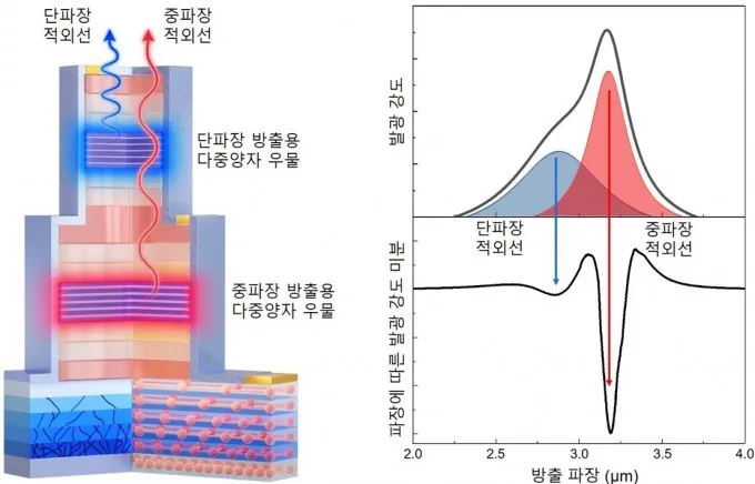
Structure of the multi-band LED stacked on a single chip (left) and its emission wavelength measurement results (right). By stacking different quantum well layers in the lower and upper sections, it simultaneously emits 2.87-micrometer (short-wavelength) and 3.18-micrometer (mid-wavelength) infrared light. Courtesy of the National Research Foundation of Korea.
Key Innovation: Compound Semiconductor Material
The breakthrough relies on a compound semiconductor material made of indium, arsenic, and antimony. The research team applied a multiple quantum well (MQW) structure, where thin layers of semiconductors are stacked alternately. This design traps electrons and generates light. By adding a small amount of antimony, they were able to adjust atomic bonds and angles, preventing common issues like lattice mismatches and defects.
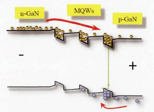 | Energy band structure of multiple quantum wells in LEDs |
Enhanced Efficiency and Light Quality
The team utilized atomic-resolution electron microscopy and AI-based simulations to confirm that adding antimony evenly distributes strain throughout the structure. This significantly reduces defects and improves light emission efficiency, allowing for a stable and high-performance LED that emits two distinct wavelengths from a single chip.
Implications and Applications
This breakthrough is expected to have wide-ranging effects across several fields:
| Biodiagnostics | More compact, cost-effective diagnostic tools. |
| Environmental Monitoring | Improved gas detection with higher accuracy. |
| Autonomous Driving | Enhanced LiDAR systems for better sensing, with a broader range of infrared light. |
By emitting two wavelengths from a single chip, the new technology reduces sensor size and complexity, making them more affordable and easier to integrate.

