


Summary :TSMC’s mass production of its COUPE photonic engine, integrated with its “Three-Layer Cake” strategy, sets a new global benchmark in high-speed optical interconnects and post-Moore semiconductor innovation.
Taiwan Semiconductor Manufacturing Company (TSMC) has begun mass production of its self-developed COUPE compact universal photonic engine, marking a major milestone in high-speed optical interconnects. As the world’s only commercially deployed Co-Packaged Optics (CPO) solution, COUPE integrates cross-generational performance advantages with a proprietary optoelectronic architecture, positioning TSMC at the forefront of global semiconductor innovation.
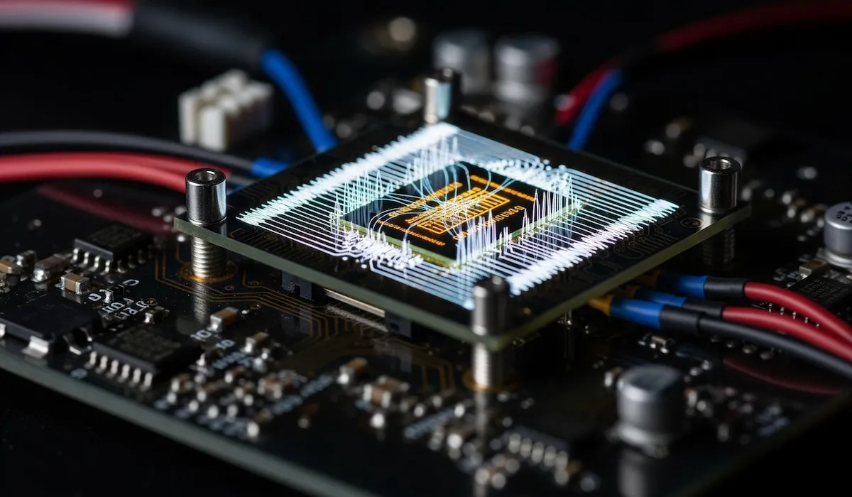
TSMC’s “Three-Layer Cake” strategy divides innovation into three complementary layers: advanced process nodes, advanced packaging, and system- and platform-level integration. Advanced process nodes focus on improving transistor performance and energy efficiency at smaller geometries. Advanced packaging combines multiple chips through 3D stacking or system-in-package techniques, enhancing density, connectivity, and signal integrity. System-level integration optimizes entire modules and platforms, enabling high-performance computing systems and AI servers with fully integrated architectures.

COUPE exemplifies the synergy between these layers. Using TSMC’s SoIC-X 3D copper-to-copper bonding, COUPE vertically integrates 6/7nm electronic circuits with 65nm silicon photonic chips. Signal paths shrink from millimeters to microns, enabling single-channel transmission rates of 200Gbps, reducing power consumption by 70–80%, and cutting latency by up to 90%, while dramatically increasing bandwidth density.
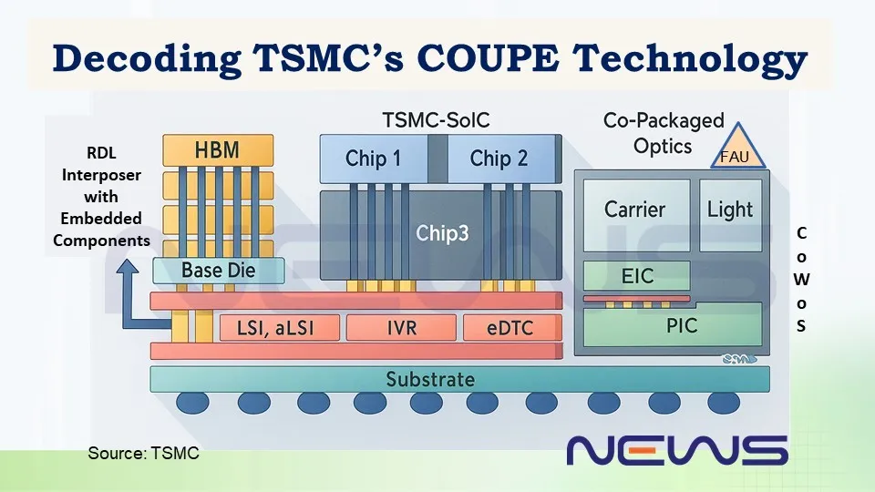
By linking COUPE with the three-layer framework, TSMC reinforces each layer: advanced nodes deliver high-performance chips, 3D packaging merges photonics and electronics into a single module, and system-level integration enables full optical interconnects, redefining AI server and supercomputing architectures. Unlike competitors such as Intel and Samsung, which remain in lab or prototype stages, TSMC has completed validation, yield ramp-up, and large-scale production, maintaining both technological and commercial leadership.
Industry experts note that combining COUPE with the “Three-Layer Cake” strategy signals a new era of optoelectronic convergence. As production scales, this integrated approach is expected to drive AI computing, cloud data centers, high-speed communications, autonomous vehicles, and next-generation digital infrastructure, establishing TSMC as a global benchmark in semiconductor innovation.

