


Summary:Japan’s newly unveiled sub-2nm transistor insulation technology enables atomic-scale device control, paving the way for faster, more energy-efficient chips and future semiconductor scaling beyond 2nm.
June 10, 2026 — Japanese researchers have announced a major breakthrough in semiconductor technology, developing a transistor gate-insulator structure that could support chip scaling beyond the 2-nanometer era. The innovation reduces the silicon oxide interface layer to just 0.2 nanometers—approximately a single atomic layer—while introducing a novel dipole-layer material that significantly improves transistor threshold voltage control.
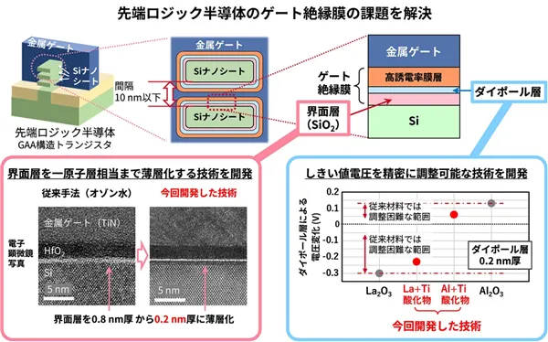
The technology addresses one of the most critical challenges facing advanced semiconductor manufacturing: maintaining performance gains while reducing power consumption as transistors continue to shrink. By enabling atomic-scale control of transistor behavior, the new gate-insulator architecture provides greater flexibility in balancing speed, efficiency, and reliability.
The breakthrough is particularly important for Gate-All-Around (GAA) transistors, which are expected to become the foundation of future logic chips. Researchers report that the design achieves an equivalent oxide thickness of approximately 0.9 nanometers without sacrificing device stability, allowing further miniaturization while preserving electrical performance.
Industry experts believe the development could help extend semiconductor scaling beyond current 2nm roadmaps. Improved gate control can increase transistor density, reduce leakage current, enhance thermal efficiency, and improve overall chip performance. These advantages are expected to benefit a wide range of applications, including artificial intelligence processors, high-performance computing systems, data centers, and next-generation mobile devices.
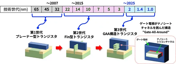
As the semiconductor industry approaches the physical limits of conventional transistor design, advances in materials engineering are becoming increasingly important. Japan’s latest achievement demonstrates how atomic-level innovation can unlock new pathways for chip development, potentially accelerating the transition toward sub-2nm technologies and shaping the next generation of computing hardware.

