


Abstract:TSMC, imec, and ASML have demonstrated wafer-scale 2D atomic transistor arrays on a 300mm platform, highlighting a promising post-silicon CMOS path for ultra-low-power computing.

In June 2026, TSMC, imec, and ASML jointly announced a major semiconductor breakthrough: the successful wafer-scale integration of two-dimensional (2D) atomic-layer transistors on a standard 12-inch (300mm) silicon platform. This represents one of the first CMOS-compatible demonstrations of atomically thin semiconductor devices at industrial wafer scale.
The transistors are based on monolayer transition metal dichalcogenides (TMDs), including MoS₂ and WSe₂, with a channel thickness of approximately 0.6–0.8 nanometers, effectively a single atomic layer. This extreme scaling provides near-ideal electrostatic gate control, significantly suppressing short-channel effects that limit advanced silicon technologies.
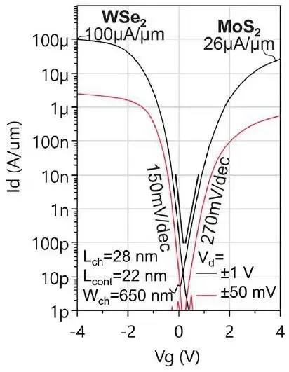
The team successfully fabricated both n-type and p-type devices and integrated them into CMOS-compatible arrays with a contacted poly pitch of around 50nm. The process is designed for compatibility with existing semiconductor manufacturing ecosystems, including 300mm wafer production lines and advanced lithography infrastructure.
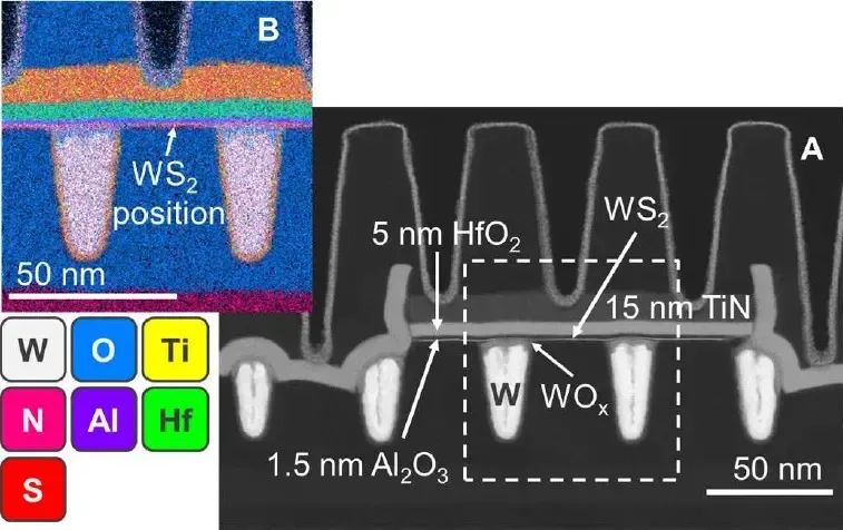
A key highlight is the reported device performance improvement in power efficiency. Compared with advanced silicon FinFET and gate-all-around (GAA) transistors, the 2D architecture demonstrates over 90% reduction in leakage current, significantly lowering static power consumption and heat generation—two critical bottlenecks for AI chips and high-performance computing systems.
In addition, the wafer-scale process achieved approximately 94% functional yield, a critical milestone that indicates early-stage manufacturability beyond laboratory demonstration. This suggests the technology is moving closer to potential industrial adoption rather than remaining purely experimental.
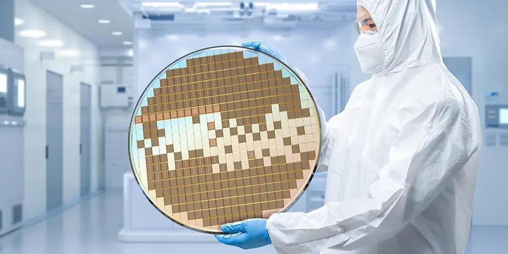
The fabrication process also operates at relatively low thermal budgets, enabling compatibility with 3D chip stacking, heterogeneous integration, and advanced packaging techniques. These characteristics make it suitable for future AI accelerators, edge computing hardware, and compact intelligent systems where energy efficiency and thermal constraints are increasingly important.
Overall, industry observers consider 2D atomic transistors a leading candidate for post-silicon logic, alongside CFET vertical architectures and other advanced nanosheet technologies. If scalable, the approach could redefine future semiconductor roadmaps for ultra-low-power and high-density computing.

