


Summary: Intel is advancing semiconductor scaling with its Hyper-Large Form Factor (HLFF) advanced packaging technology, developed at Intel Foundry’s Rio Rancho, New Mexico facility. Combining EMIB and Foveros packaging technologies, the platform enables ultra-large chip architectures beyond 12× reticle size, opening new possibilities for AI processors, high-performance computing, and next-generation semiconductor systems.
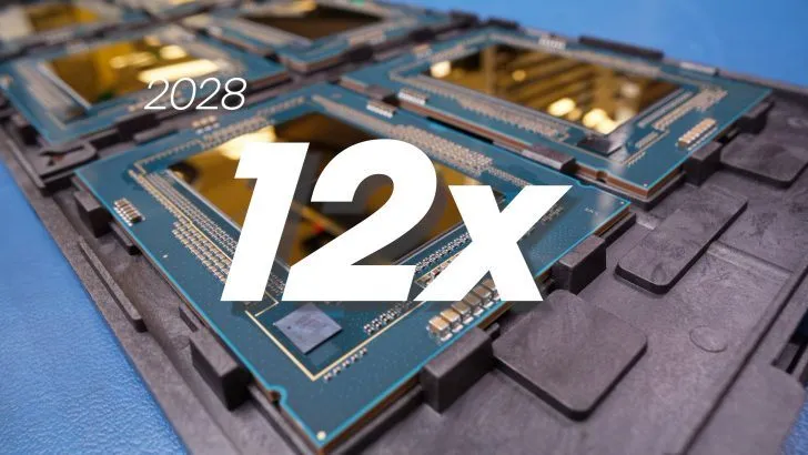
Intel Foundry is pushing the boundaries of semiconductor manufacturing with its Hyper-Large Form Factor (HLFF) advanced packaging technology, a new approach designed to overcome the scaling limitations of traditional single-die chips.
Developed at Intel’s Rio Rancho, New Mexico advanced packaging facility, HLFF technology transforms modern processors into large-scale “silicon mosaics” by integrating multiple specialized chiplets into a single high-performance package.
The technology builds on Intel’s advanced packaging platforms, including EMIB (Embedded Multi-die Interconnect Bridge) and Foveros 3D packaging, allowing chip designers to combine computing tiles, high-bandwidth memory, and specialized accelerators in larger and more efficient architectures.
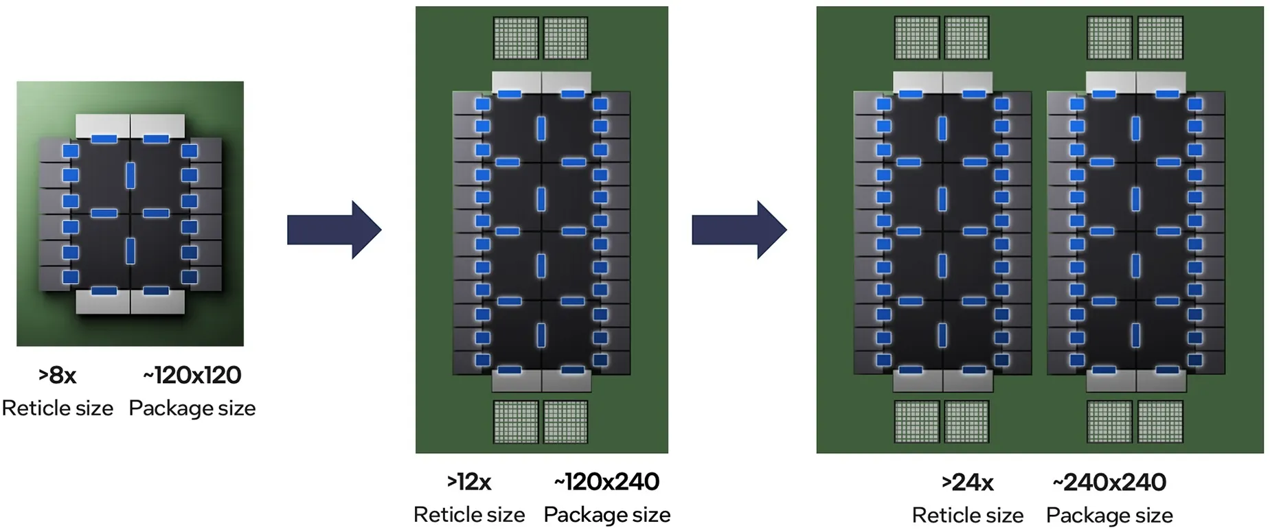
Intel’s HLFF roadmap targets ultra-large packages measuring 240 mm × 240 mm, reaching approximately 24× reticle size. The company is developing solutions designed to support chip packages beyond 12× reticle size by 2028, enabling significantly higher computing density for artificial intelligence and data center applications.
Scaling these massive chip packages requires breakthroughs in materials, power delivery, thermal management, and manufacturing reliability. Intel has developed advanced encapsulation technologies that combine optimized underfill materials, multi-point dispensing methods, and improved curing processes to achieve reliable, void-free packaging at larger dimensions.
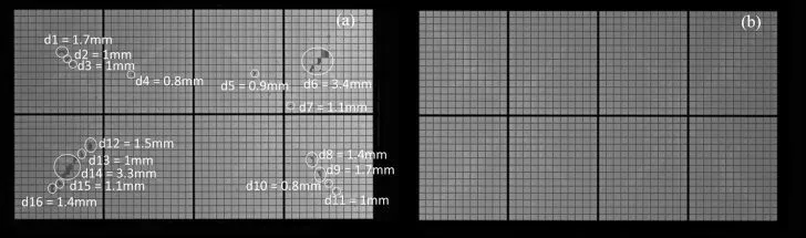
The company has successfully validated EMIB-based packages exceeding 5× reticle size, integrating 18 dies with 12 HBM memory sites, while achieving void-free encapsulation across flow distances of up to 40 mm. Intel has also demonstrated larger tiled EMIB packages beyond 7× reticle size and validated Foveros-based 3D packaging at multiple reticle scales.
Future HLFF packages are expected to address the growing demand for AI computing power, where traditional chip scaling alone can no longer meet performance requirements. By combining chiplets, advanced interconnect technologies, and large-scale packaging, Intel aims to create a new generation of high-performance processors with improved scalability and efficiency.

