


Summary:TSMC and National Yang Ming Chiao Tung University have developed an atomic-scale interface engineering technology that significantly improves single-layer MoS₂ transistors, opening a new pathway for sub-1nm semiconductor chips.
A breakthrough in two-dimensional semiconductor technology may accelerate the future of sub-1nm chip manufacturing. TSMC and researchers from National Yang Ming Chiao Tung University have developed an advanced epitaxial interface engineering technology that dramatically improves the performance of single-layer molybdenum disulfide (MoS₂) top-gate transistors.
Published in Nature Electronics, the research introduces a 0.42nm aluminum oxide (Al₂O₃) atomic-scale buffer layer between the MoS₂ channel and high-k hafnium oxide (HfO₂) gate dielectric. This ultra-thin interface structure solves one of the biggest challenges in 2D semiconductor devices: defects and electron scattering at the channel-dielectric interface.
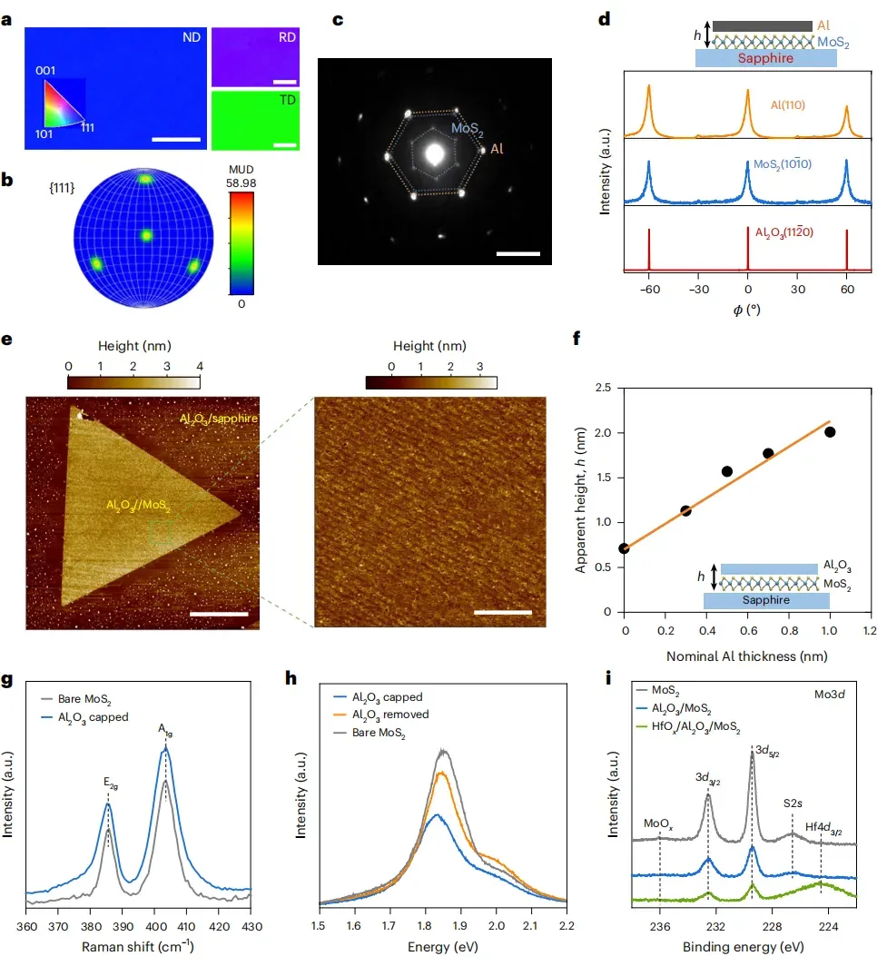
Subnanometer alumina epitaxially derived on a monolayer of molybdenum disulfide
Unlike traditional silicon materials, MoS₂ has a chemically inert surface, making it difficult to directly integrate with conventional gate dielectrics. The newly developed interface engineering approach creates a more stable atomic connection, improving electrical control and reducing performance losses.
The resulting MoS₂ top-gate transistor achieved a peak transconductance of 0.45 mS/μm, an on-state current of 0.45 mA/μm, and a subthreshold swing of 75 mV/dec, representing a major advance for CVD-grown single-layer MoS₂ devices.
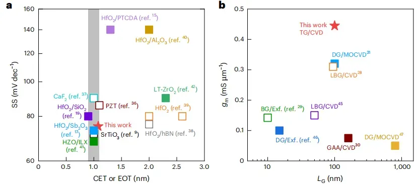
Comparison of device performance benchmarks.
The technology is designed to be compatible with existing semiconductor manufacturing processes, including EUV lithography and advanced thin-film deposition. It could provide a practical route toward future angstrom-scale chips, AI processors, and ultra-low-power semiconductor devices.
While large-scale wafer integration and manufacturing yield remain challenges, this interface engineering breakthrough marks an important step toward bringing two-dimensional materials from laboratory research into next-generation semiconductor production.

