


Summary: TSMC and National Yang Ming Chiao Tung University (NYCU) have solved one of the biggest barriers to commercial 2D semiconductors, opening a potential path beyond silicon for future AI processors and sub-1nm chips.
The semiconductor industry has spent years searching for a successor to silicon as transistor scaling approaches fundamental physical limits. Now, TSMC and NYCU have reported a major breakthrough that could accelerate the transition to next-generation semiconductor technology.
Published in Nature Electronics, the research demonstrates a high-performance monolayer molybdenum disulfide (MoS₂) transistor enabled by an advanced interface engineering technique. While 2D semiconductor materials have long been viewed as a promising candidate for sub-1nm chips, commercialization has been hindered by a critical challenge: poor interfaces between ultra-thin semiconductor layers and surrounding insulating materials.
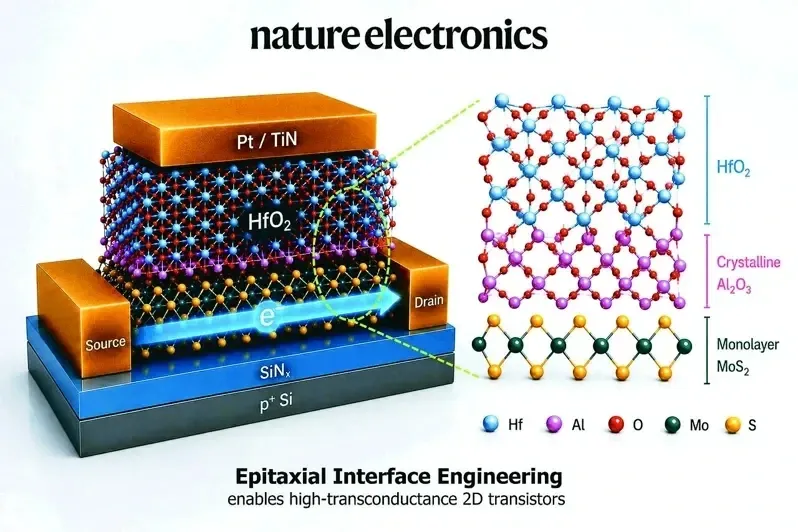
The TSMC-led team addressed this bottleneck by creating an atomically smooth 0.42-nanometer aluminum oxide interface layer under ultra-high-vacuum conditions. The engineered interface dramatically reduces defects, minimizes carrier scattering, and preserves electron mobility—factors essential for maintaining performance at extreme transistor dimensions.
The achievement is significant because interface quality, rather than the semiconductor material itself, has become one of the largest obstacles to extending Moore’s Law. Industry experts increasingly believe that future technologies such as CFET (Complementary FET) architectures and sub-1nm process nodes will require 2D materials to overcome leakage current and power-efficiency limitations facing conventional silicon devices.
Performance results underscore the advance. The new transistor achieved a transconductance of 0.45 mS/μm at an equivalent oxide thickness of just 1nm while maintaining low leakage current and strong operational stability. Equally important, the process is compatible with existing semiconductor manufacturing infrastructure, potentially reducing barriers to large-scale adoption.
The broader impact extends far beyond a single transistor design. As AI models continue to drive demand for higher computing performance and lower energy consumption, breakthroughs in 2D semiconductor integration could become a foundation for future AI accelerators, mobile processors, high-performance computing systems, and data-center hardware.
For the semiconductor industry, this development signals a shift in competition—from shrinking silicon transistors to mastering new materials and interface engineering. If successfully commercialized, the technology could help define the post-silicon era and extend the roadmap for advanced semiconductor innovation well beyond today's leading-edge nodes.

