


Abstract:A new fabrication strategy reported in Science Advances combines wafer-scale tungsten diselenide (WSe₂) growth with an ultrathin tungsten oxide (WOₓ) buffer layer to improve p-type transistor performance. By protecting the semiconductor channel during dielectric deposition, the approach offers a potential route toward more densely integrated two-dimensional CMOS circuits.
The semiconductor industry is approaching a stage where improving transistor performance depends not only on shrinking conventional silicon devices, but also on developing new materials and integration methods. Two-dimensional (2D) transition metal dichalcogenides (TMDs), including tungsten diselenide (WSe₂), are attracting attention because they can retain useful electronic properties at atomic-scale thicknesses. Yet a major obstacle remains: producing reliable p-type transistors that can be integrated into practical complementary metal-oxide-semiconductor (CMOS) circuits.
Researchers reporting in Science Advances have addressed this challenge through a combination of wafer-scale material synthesis and interface engineering. Their work focuses on WSe₂, a semiconductor suited to p-type operation, and a tungsten oxide (WOₓ) buffer layer designed to protect the channel during device fabrication.
The process begins with metal-organic chemical vapor deposition (MOCVD), which produces uniform WSe₂ films on two-inch silicon wafers at approximately 580°C. The researchers also optimized the growth conditions to suppress carbon contamination and enlarge the material’s crystalline grains. This is important because defects and nonuniformity can undermine electrical performance when semiconductor materials are manufactured across large areas.
The second innovation is the WOₓ buffer layer. During conventional atomic layer deposition (ALD), used to form the gate dielectric, direct exposure can damage WSe₂ and introduce unwanted n-type doping. The researchers inserted an ultrathin, insulating WOₓ layer between the channel and the aluminum oxide gate dielectric. This interface helps preserve the channel’s properties, promotes hole conduction and reduces electrical charge trapping.
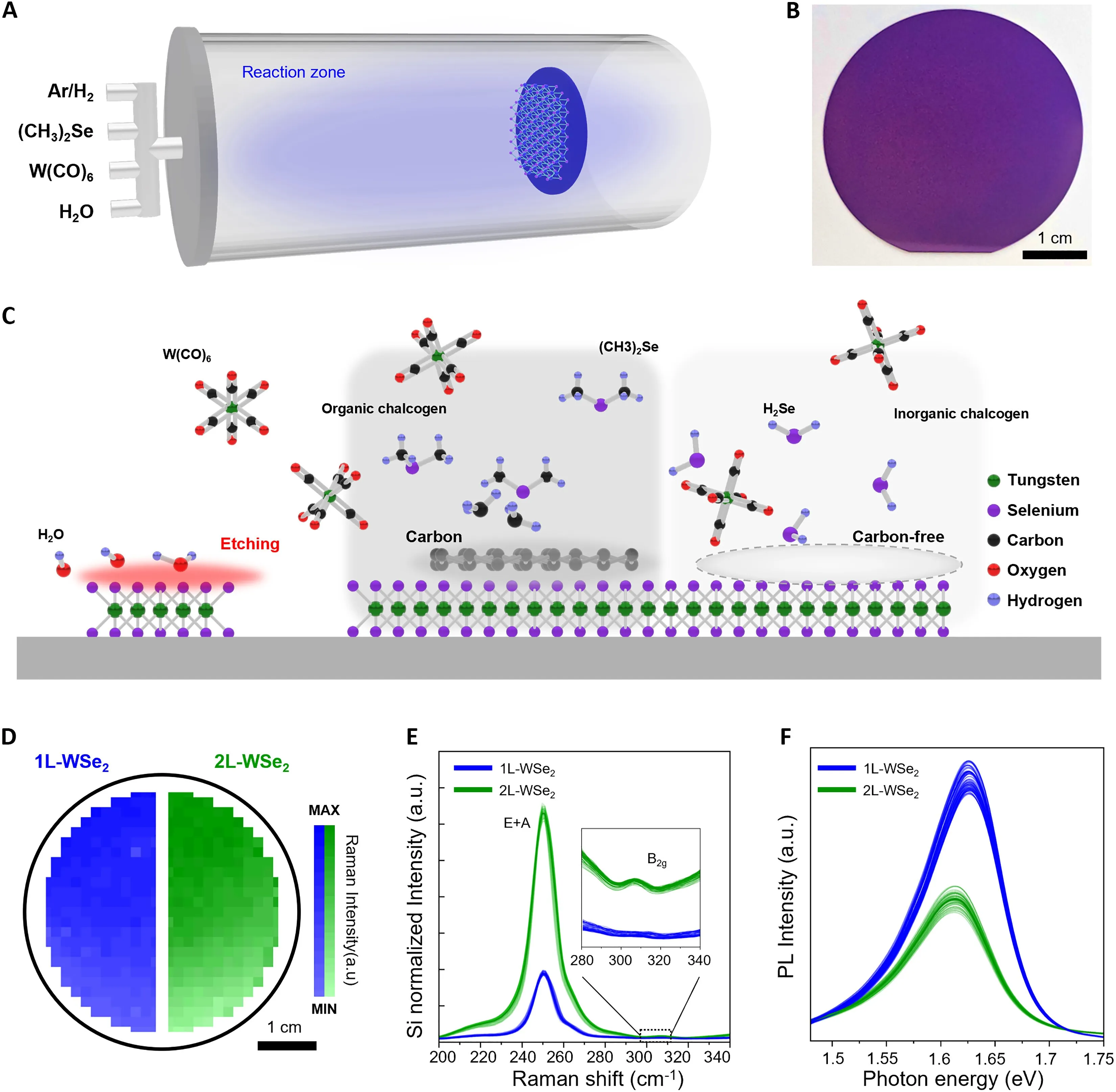
Figure 1, Wafer-scale synthesis of highly uniform WSe₂ films via MOCVD.
The electrical results demonstrate the significance of this approach. The top-gate field-effect transistors achieved an average hole mobility of 10.49 ± 2.35 cm² V⁻¹ s⁻¹, reaching a maximum of 15.63 cm² V⁻¹ s⁻¹. Their on/off current ratio reached approximately 2.4 × 10⁹, while the subthreshold swing improved to 140.43 ± 13.67 mV per decade.
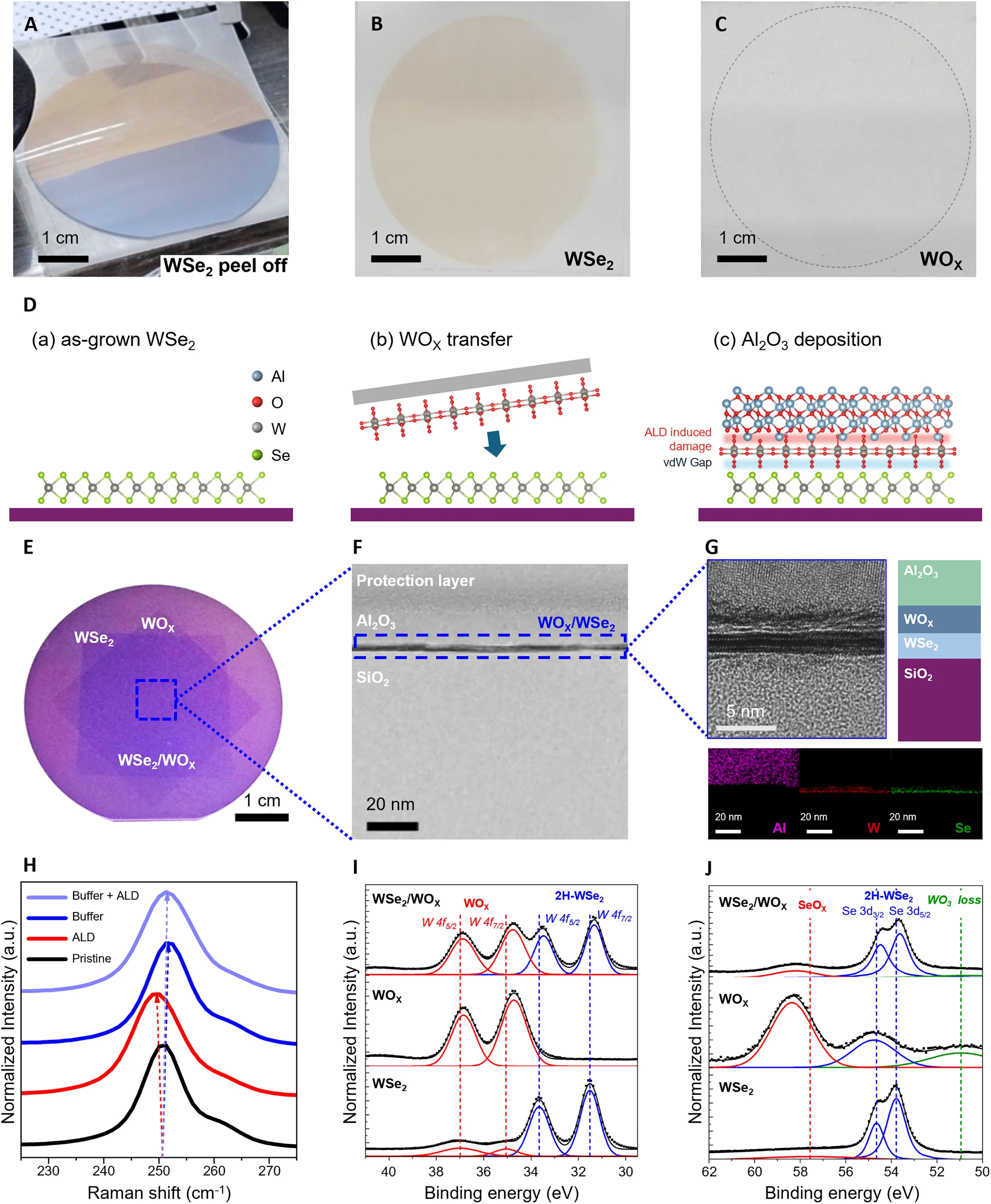
Figure 2, Preparation of the WOₓ buffer layer.
Importantly, the team moved beyond individual transistors to demonstrate functional PMOS logic circuits, including NOT, NAND, NOR, AND and OR gates. Their switching responses remained stable at measured frequencies up to 10 kHz, showing that the material and fabrication strategy can support basic circuit-level operation.
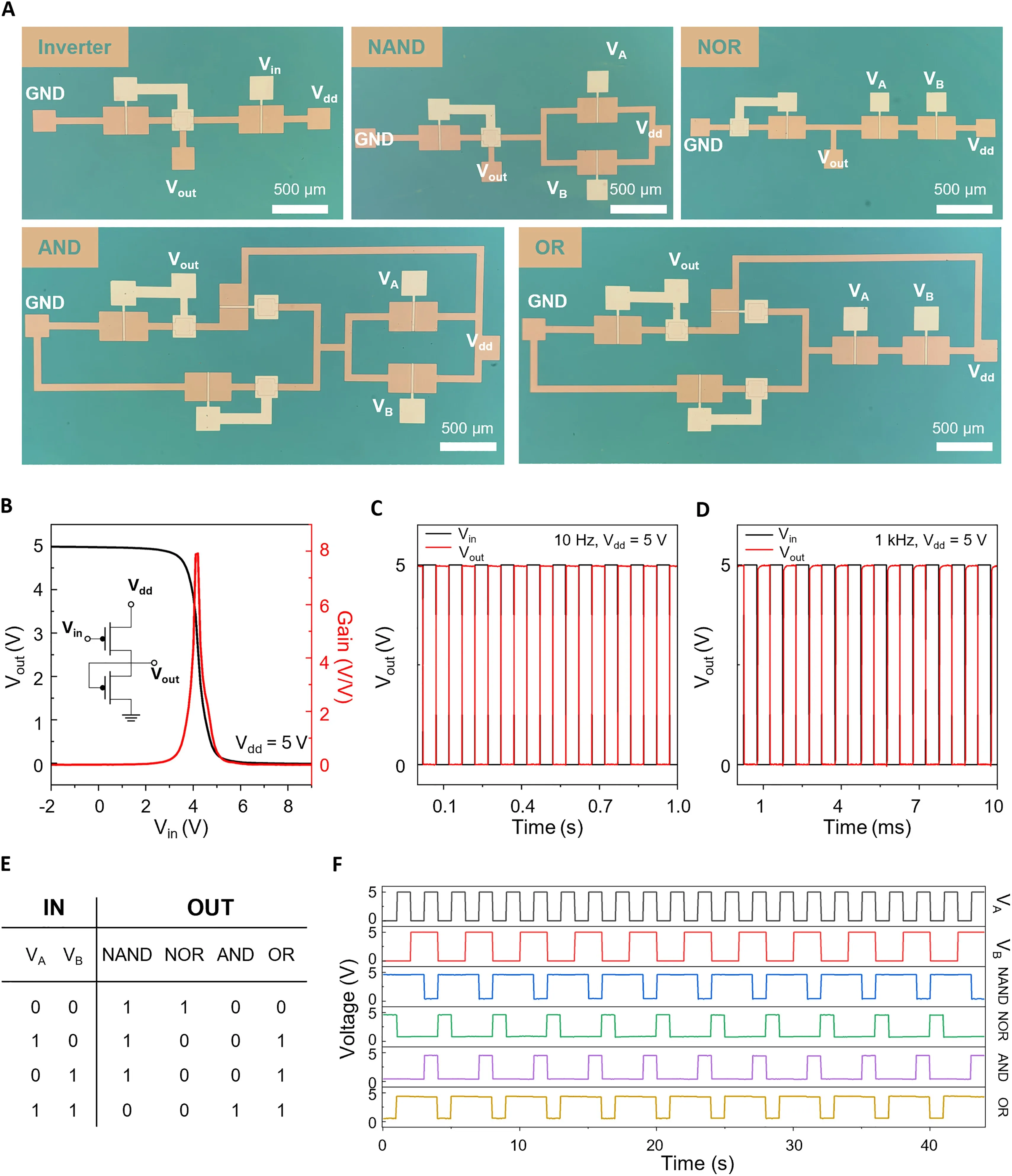
Figure 4, PMOS logic circuits based on wafer-scale WSe₂ FETs.
The broader significance lies in the potential to integrate atomically thin semiconductors into high-density CMOS logic and, eventually, monolithic three-dimensional chip architectures. Reliable p-type devices are essential for balancing the n-type transistors already developed from other 2D materials.
However, the demonstrated two-inch wafer process is still a research-stage technology. Scaling to larger wafers, improving manufacturing yield and reliability, and meeting commercial requirements for speed and power efficiency remain important challenges. If these hurdles can be overcome, the WOₓ-buffer strategy could help bring 2D semiconductor electronics closer to practical manufacturing.

